PN Junction: Why 0.7 V Isn't the Barrier Potential
One number runs through almost every set of notes on the pn junction: 0.7 V for silicon.

By Rahul Jeewani, Founder · Updated 2 Nov 2026

Key takeaways
- The barrier potential (also called the built-in potential, V₀) and the 0.7 V cut-in voltage are different quantities. In our calculation V₀ for silicon runs from about 0.6 V to 1.07 V with doping, while the National Council of Educational Research and Training (NCERT) gives about 0.7 V as silicon's cut-in voltage.
- A silicon diode has no fixed forward voltage: it rises with the current the diode carries.
- A voltmeter cannot read V₀, and reverse current is tiny because only minority carriers cross a barrier that reverse bias has raised.
- In an exam, find the word first (barrier, cut-in or drop). Then use the value the question or your textbook gives.
In this article
- 1What is a pn junction and where does the barrier potential come from?
- 2Which 0.7 V is your pn junction question asking about?
- 3How much does the built-in potential of a silicon pn junction change with doping?
- 4Why does a silicon diode not stay at 0.7 V when the current rises?
- 5Can a voltmeter read the barrier, and why is reverse current so small?
- 6How should you answer pn junction questions in HSC, MHT-CET and FE Physics?
- 7Where do we teach the pn junction at RG Lectures?
- 8Frequently asked questions
It is called the barrier potential in one line, the cut-in voltage in the next, and the voltage drop in a circuit sum after that. These are three different quantities that happen to share a figure.
Students preparing for the Higher Secondary Certificate (HSC) exams, the Maharashtra Common Entrance Test (MHT-CET) or first-year engineering (FE) run into this in the same few ways. If the barrier is 0.7 V, why does the diode not stop at 0.7 V when the supply goes higher? Why does current seem to start only after 0.7 V? Can a voltmeter across the junction read the barrier?
Each question has a short answer once you know which quantity it means. This page separates the three and gives you a table to decide which one you are being asked.
What is a pn junction and where does the barrier potential come from?
A pn junction is the boundary inside one crystal where p-type material, with holes as the majority carriers, meets n-type material, with electrons as the majority carriers. Electrons and holes diffuse across, leaving fixed charged ions behind, and the field of those ions stops the crossing. The potential across that region is the barrier potential.
Pn junctions sit inside solar cells, light-emitting diodes and diode lasers, and they are present in all types of transistors.
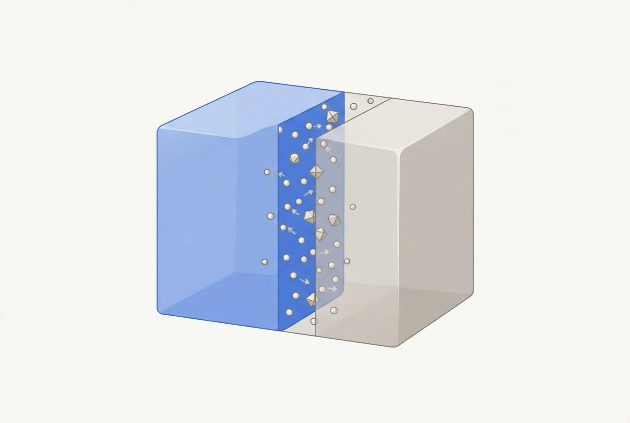
Both types come from doping, which means adding a small amount of impurity atoms to a pure semiconductor such as silicon. When the two meet, electrons cross into the p side and holes into the n side. The n side near the junction is left with fixed positive ions and the p side with fixed negative ions. This stripped layer is the depletion region, of the order of one-tenth of a micrometre thick.
Why does the crossing stop? Each electron that leaves the n side uncovers a fixed positive donor ion, and each hole that leaves the p side uncovers a fixed negative acceptor ion. The field of these ions grows until the drift current it causes equals the diffusion current. The potential across the depletion region at that balance is the barrier potential, also written V₀.
Which 0.7 V is your pn junction question asking about?
It depends on the words in the question. "Barrier potential" or "built-in potential" means V₀, which you calculate from doping. "Threshold", "cut-in" or "knee" means the rule-of-thumb voltage after which current rises sharply. "Voltage drop" in a circuit means the forward voltage at the current in the circuit.
| Question words | Quantity | Value to write | What it depends on | Source |
|---|---|---|---|---|
| Barrier potential, built-in potential, V₀ | Built-in potential | About 0.6 V to 1.1 V for silicon | Doping and temperature | Hu, section 4.1.2, table below |
| Threshold, cut-in, knee voltage | Cut-in voltage | About 0.7 V silicon; about 0.2 V germanium in NCERT (many other Indian notes use 0.3 V) | The current you treat as "on" | |
| Voltage drop across a conducting diode | Forward voltage, V_F | 0.7 V in a sum; the datasheet value in design | Current through the diode | |
| Thickness of the depletion layer | Depletion width | About 0.1 µm | Doping and bias |
For silicon the three voltages sit close together, between roughly 0.6 V and 1 V. That is why they get swapped. Only V₀ belongs to the junction itself. The other two move with the current you ask the diode to carry.
How much does the built-in potential of a silicon pn junction change with doping?
It changes a lot: in our calculation it runs from about 0.6 V to 1.07 V across doping levels from 10¹⁵ to 10¹⁹ per cm³. The built-in potential is V₀ = (kT/q) ln(NₐN_d / nᵢ²), where Nₐ and N_d are the acceptor and donor doping and nᵢ is the intrinsic carrier concentration (Hu, section 4.1.2, Eq. 4.1.2).
Our method: T = 300 K, so kT/q = 0.02585 V, and we took silicon nᵢ = 1×10¹⁰ per cm³ (our assumption, not a quoted constant). Doping is equal on both sides.
| Doping on each side (per cm³) | Built-in potential V₀ |
|---|---|
| 10¹⁵ | 0.60 V |
| 10¹⁶ | 0.71 V |
| 10¹⁷ | 0.83 V |
| 10¹⁸ | 0.95 V |
| 10¹⁹ | 1.07 V |
Worked row, 10¹⁶ on both sides: ln(10³² / 10²⁰) = ln(10¹²) = 27.63, and 27.63 × 0.02585 V = 0.714 V. Each tenfold rise in doping on both sides adds ln(100) × 0.02585 = 0.119 V.
Hu puts a typical silicon V₀ at about 0.9 V (section 4.1.2), which sits inside the range of our table. With nᵢ = 1.5×10¹⁰ every value in our table falls by about 0.02 V. The 0.7 V figure shows up at 10¹⁶ doping, and that is a coincidence of the numbers, not a rule.
Why does a silicon diode not stay at 0.7 V when the current rises?
Because the forward voltage depends on current. For the diode in NCERT exercise 14.10, the ideal equation gives about 0.55 µA at 0.3 V, but about 60 mA at 0.6 V and about 2.9 A at 0.7 V. Current multiplies about 48 times for each extra 0.1 V.
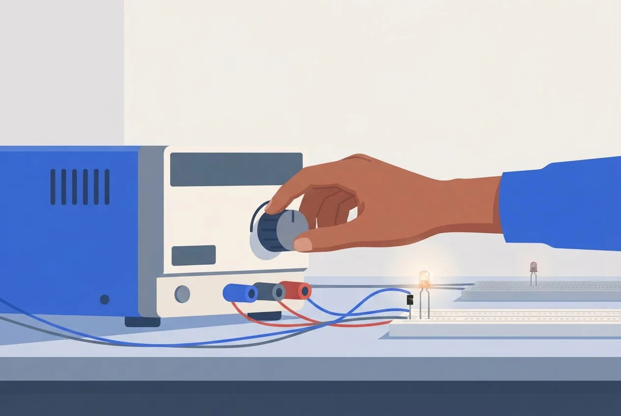
Our working: I = I₀(e^(V/V_T) − 1), with I₀ = 5×10⁻¹² A and T = 300 K as the NCERT exercise gives them, and V_T = kT/q = 0.02585 V.
| Forward voltage | Current from the ideal equation |
|---|---|
| 0.3 V | about 0.55 µA |
| 0.4 V | about 26 µA |
| 0.5 V | about 1.25 mA |
| 0.6 V | about 60 mA |
| 0.7 V | about 2.9 A |
This is the ideal equation, and real diodes follow it only roughly. Treat the table as a pattern, not a prediction for a particular part.
Datasheets quote a forward voltage at a stated current, not a flat 0.7 V. Vishay’s 1N4148 datasheet (revision 1.6, 7 November 2024) gives a maximum of 1 V at 10 mA, and its Fig. 2 plots forward current against forward voltage for that one diode. Vishay’s 1N4001 to 1N4007 datasheet (29 April 2020) gives a maximum of 1.1 V at 1.0 A for a larger rectifier diode.
An exponential looks like a knee on a linear graph. At 0.6 V the minority-carrier density at the edge of the depletion region is already about 10¹⁰ times higher (Hu, section 4.6, Eq. 4.6.2). Current flows long before the applied voltage reaches V₀. Under forward bias the barrier height becomes (V₀ − V) (NCERT).
Our advice: use 0.7 V in a textbook circuit sum, and read the datasheet curve at your actual current when you design something.
Can a voltmeter read the barrier, and why is reverse current so small?
No, a voltmeter reads nothing across a bare junction. The built-in potential at the junction is cancelled by the potentials at the semiconductor-metal contacts and wire joins, so the sum around the closed loop is zero (Hu, section 4.1.2). The field is still real, and it accelerates carriers.
Reverse current is small because reverse bias raises the barrier from V₀ to V₀ + V_r and widens the depletion layer. Only minority carriers (electrons on the p side, holes on the n side) can then cross, and there are few of them (Hu, section 4.3). The result is a reverse saturation current of the order of a microampere, almost constant until breakdown (NCERT).
| Bias | Barrier height | Depletion layer | Current |
|---|---|---|---|
| Zero bias | V₀ | Equilibrium width | Drift and diffusion currents balance, so the net current is zero |
| Forward bias | V₀ − V | Narrower | Rises exponentially with V |
| Reverse bias | V₀ + V_r | Wider | Tiny, because only minority carriers cross |
How should you answer pn junction questions in HSC, MHT-CET and FE Physics?
Name the quantity first, then pick the number. Run these five checks before you write a value.
- Find the wordUnderline barrier, built-in, cut-in, knee or drop. Pass: you can say which row of the table above you are in before you write any number.
- A given value existsIf the question gives a voltage or a current, use it. Pass: the number you use appears in the question or your textbook. If your textbook or the question calls 0.7 V the barrier potential, write the textbook's number for the marks, and know the difference.
- The question is silentIf no value is given, use the cut-in values in your own textbook. NCERT gives about 0.7 V for silicon and about 0.2 V for germanium, while many Indian notes and answer keys use 0.3 V for germanium. Pass: you wrote your textbook’s value and called it the cut-in voltage.
- Apply the bias correctly
Forward bias gives a barrier of (V₀ − V). Reverse bias gives V₀ + V_r, with a wider depletion layer. Pass: your barrier goes down in forward bias and up in reverse bias.
- Check any statement about a voltmeterPass: you write that the contact potentials cancel the built-in potential, so the meter reads 0 V. Fail: you write that it reads V₀.
The formulas for this topic (V₀, the diode equation and the bias rules) are on this page. For the other HSC chapters, our HSC Physics formula sheet for Maharashtra Class 12 lists them chapter by chapter.
Where do we teach the pn junction at RG Lectures?
We teach it in our first-year engineering Physics courses and in our MHT-CET 2027 batch. Padhna Aasaan Hai, and for the pn junction that means building up from energy bands and doping before the diode, so the barrier makes sense and 0.7 V is not just a number to memorise.
Our Engineering Physics courses for Pune University and Mumbai University (2026-27) are taught in Hindi by RG Sir and come as pre-recorded lectures with notes. As of November 2026 each costs ₹1,299 (MRP ₹1,599). The Pune course lists lectures on the effect of doping and temperature, then "PN Junction Diode" and "Applications of Pn Junction Diode"; the Mumbai course lists the same two diode lectures. To pick the course that matches your syllabus, start with our guide to Engineering Physics 1 or our comparison of Engineering Physics course options.
The MHT-CET 2027 batch costs ₹1,632 (MRP ₹1,999) as of November 2026. It covers the full MHT-CET syllabus and combines live and recorded classes.
See both in the RG Lectures store.
Learn the pn junction the Padhna Aasaan Hai way
Frequently asked questions
Sources
- 1.NCERT, Class 12 Physics Part II, Chapter 14, Semiconductor Electronics (2020-21 edition)
- 2.Chenming Hu, Modern Semiconductor Devices for Integrated Circuits, Chapter 4, PN and Metal-Semiconductor Junctions (2009), hosted by UC Berkeley
- 3.Vishay Semiconductors, 1N4148 datasheet, revision 1.6, 7 November 2024
- 4.Vishay General Semiconductor, 1N4001 to 1N4007 datasheet, 29 April 2020
- 5.RG Lectures course page: Engineering Physics, Pune University (2026-27)
- 6.RG Lectures course page: Engineering Physics, Mumbai University (2026-27)
- 7.RG Lectures course page: MHT-CET 2027 Long Term Batch
- 8.Semiconductor Industry Association, Global Annual Semiconductor Sales Increase 25.6% to $791.7 Billion in 2025, 6 February 2026